
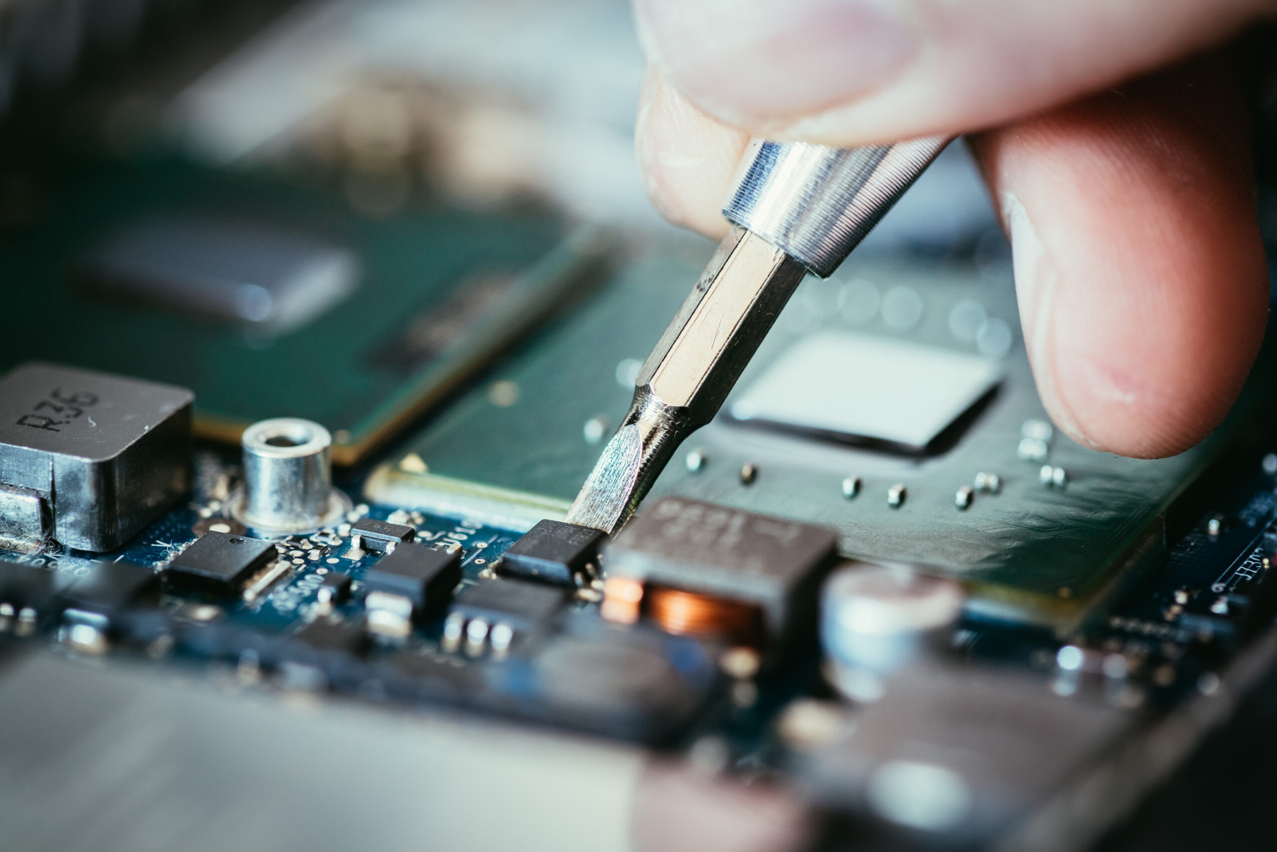
PCB Design Services — From Concept to Production-Ready Files
Whether you have a rough schematic on paper or a partial design that needs refinement, our engineering team takes your idea through every stage — schematic capture, component selection, multi-layer PCB layout, and DFM optimization — delivering clean, factory-ready output files.
We work with all major EDA tools including Altium Designer, KiCad, and Eagle, and output complete Gerber packages with BOM and assembly drawings. Every design goes through a Design for Manufacturability (DFM) check before handoff, so you avoid costly re-spins at the fabrication stage.
From single-layer hobby boards to 12-layer high-density industrial designs, we handle the full range.
Specification |
Value |
|---|---|
|
Supported layers |
1–12 layers |
|
EDA tools |
Altium Designer, KiCad, Eagle, PADS |
|
Min. trace / space |
3/3 mil |
|
Min. via size |
0.2 mm |
|
Output files |
Gerber, BOM, pick-and-place file, assembly drawing |
|
DFM check |
Included with every project |
|
Revision policy |
First revision included; additional revisions quoted separately |
|
Typical turnaround |
3–5 business days (standard); rush available |
FAQ
I only have a concept — can you design from scratch?
Yes. Send us your requirements (function, form factor, key components, power budget) and we’ll start from a blank schematic.
What files do I need to provide?
For a new design, a written brief is enough to start. For redesigns or refinements, send your existing schematic and any reference materials.
What format are the output files?
We deliver Gerber RS-274X, Excel BOM, CSV pick-and-place, and PDF assembly drawing as standard. Other formats available on request.
Does the price include revisions?
One round of revisions is included. Additional rounds are quoted case by case.
Can you also manufacture the PCB after design?
Yes — design and fabrication are both in-house. We can move directly from approved design files to production with no extra coordination needed.